

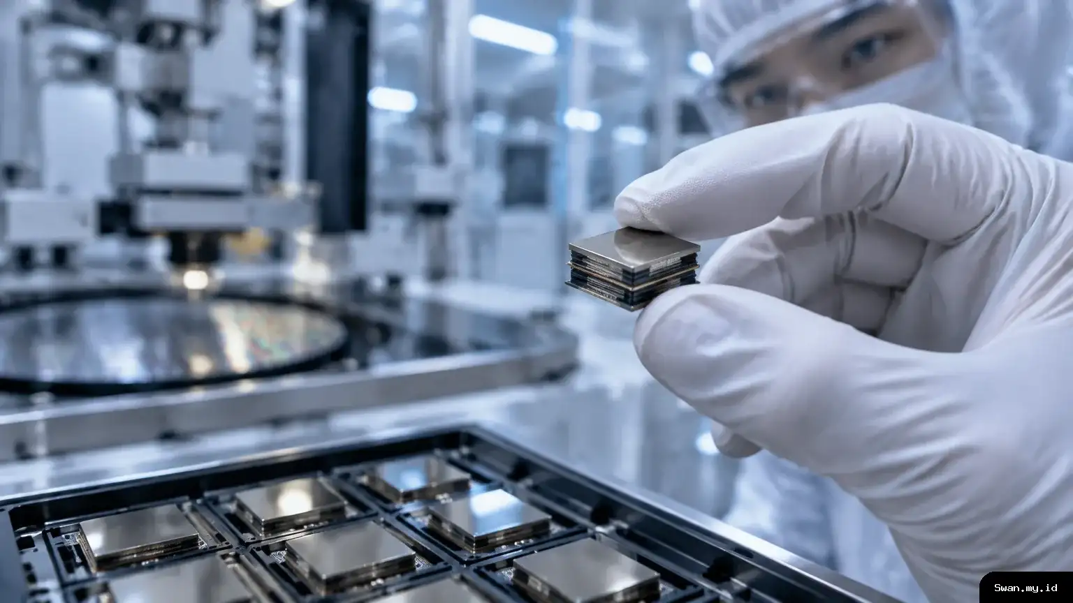
Swan.my.id - Samsung’s TSMC HBM production shift reflects a new demand from NVIDIA: suppliers must follow a common process for the base die in its next-generation memory. Samsung has agreed to use TSMC’s 3-nanometer manufacturing technology for that component, according to a Seoul Economic Daily report cited by Reuters on October 19.
The arrangement would bring Samsung and TSMC together in memory production for the first time, the report said. It also highlights how a major customer can shape the manufacturing choices of companies that otherwise compete across the semiconductor industry.
Why NVIDIA wants a shared NVHBM design
NVIDIA introduced NVHBM in August. The design places a memory controller developed by NVIDIA in the base die, the foundational chip beneath the stacked memory. This gives the company a way to standardize how the product is built across different memory suppliers.
NVIDIA has asked Samsung, SK Hynix and Micron Technology to use TSMC’s process for the NVHBM base die, while applying sixth-generation DRAM technology to the memory core, according to the report. A shared specification could make products from different suppliers more consistent for NVIDIA’s systems.
That request gives the base die a more central role than a passive foundation. It must connect the memory stack with the wider system and incorporate NVIDIA’s controller. Meanwhile, suppliers still bring their own expertise in producing the DRAM layers that store data.
Samsung agrees, but keeps other options open
Samsung accepted NVIDIA’s terms after an internal review, the report said. The decision does not mean the company will abandon its own manufacturing routes. Samsung plans to continue using its production lines for conventional HBM and customized memory products for other customers.
At the same time, Samsung is assessing whether its own foundry business could make NVHBM base dies if demand exceeds the capacity available from TSMC. That leaves the company with a potential alternative, although the report does not say Samsung has chosen to move production to its own foundry.
This distinction matters because the decision concerns a specific component and product design, not every Samsung memory chip. Samsung remains a producer of HBM, while agreeing to use a rival’s process for the NVHBM base die under NVIDIA’s requested arrangement.
What HBM does in AI systems
High-bandwidth memory, or HBM, moves data between memory and processors at very high rates. Manufacturers stack memory dies vertically and connect them closely to a processor within a compact package. The short pathways help data travel efficiently compared with conventional memory placed farther away.
AI accelerators repeatedly work with large sets of information, including model parameters and data used during training or inference. The processor can only work effectively when that information reaches it quickly. As a result, memory bandwidth can constrain overall performance even when the processor itself is powerful.
HBM helps address that bottleneck by moving large volumes of data over a short distance. Its close integration can also reduce the energy needed to move information around a system. For data centers running demanding AI workloads, those characteristics make memory a vital part of accelerator design.
However, producing HBM requires precise stacking and connections across multiple memory layers. Only a small group of manufacturers currently supplies it at commercial scale: Samsung, SK Hynix and Micron. Their output therefore matters to customers building AI chips and the systems that use them.
Customer standards reshape the supply chain
NVIDIA’s request shows how its role as a major chip customer can extend beyond choosing memory suppliers. By setting requirements for both the base die process and DRAM generation, it can influence how those suppliers organize production for a particular product.
For Samsung, the choice involves balancing customer requirements with manufacturing independence. Using TSMC’s process for this component may help meet NVIDIA’s specification, while keeping Samsung’s own lines available for other HBM products. Its review of internal foundry capacity also leaves room to respond if external production proves insufficient.
The broader pressure comes from demand for AI computing and the components needed to support it. When supply falls short of what customers need, manufacturing capacity and compatible designs become strategic concerns. In that environment, even companies with extensive production capabilities may rely on a competitor’s technology for a customer-specific part.
The reported plan does not establish how much NVHBM Samsung will produce, when manufacturing will begin, or how much capacity TSMC can provide. Still, it points to a supply chain in which control over a small but essential component can influence how quickly AI hardware reaches the market. Samsung’s agreement shows that, for NVIDIA’s next HBM design, meeting the customer’s standard comes first.
